Semiconductor
- crystalline 单晶硅: wafar
- amorphous 太阳能电池
Semiconductor Physics Recap
Semiconductor Materials
Materials with intermediate conductivity and features sensitive to physical variables.
Atomic structures:
- Crystalline: Highly ordered atomic structure, wafar
- Polycrystalline: A cluster of multiple crystalline grains.
- Amorphous: Disordered atomic structure, PV cells.
Types:
- Elemental
- IV group: Ge at first, then Si, recently C.
- Compound
- III+V group, pronounced three-five semiconductors: AsGa, AlP.
Elemental: Diamond Cubic Structure
价电子 valence electrons. 共价键 covalent bound.
Each Si atom has 4 nearest neighbors. Lattice constant: 5.431 .
Number of atoms in a unit cell:
Density of silicon atoms: 8 atoms / cell volumn = atoms/cm3.
Inpurity consentration: atoms/cm3.
Compound: Zinc Blende Structure
III-V compound. GaAs, GaP, GaN. High electron mobility, for high-speed ICs.
Crystallographic Notation
- (h k l): crystal plane 晶面,截距倒数通分取分母
- {h k l}: equivalent plane 晶面族
- [h k l]: direction
- <h k l>: equivalent direction
h: inverse x intercept. k: inverse y. l: inverse z.
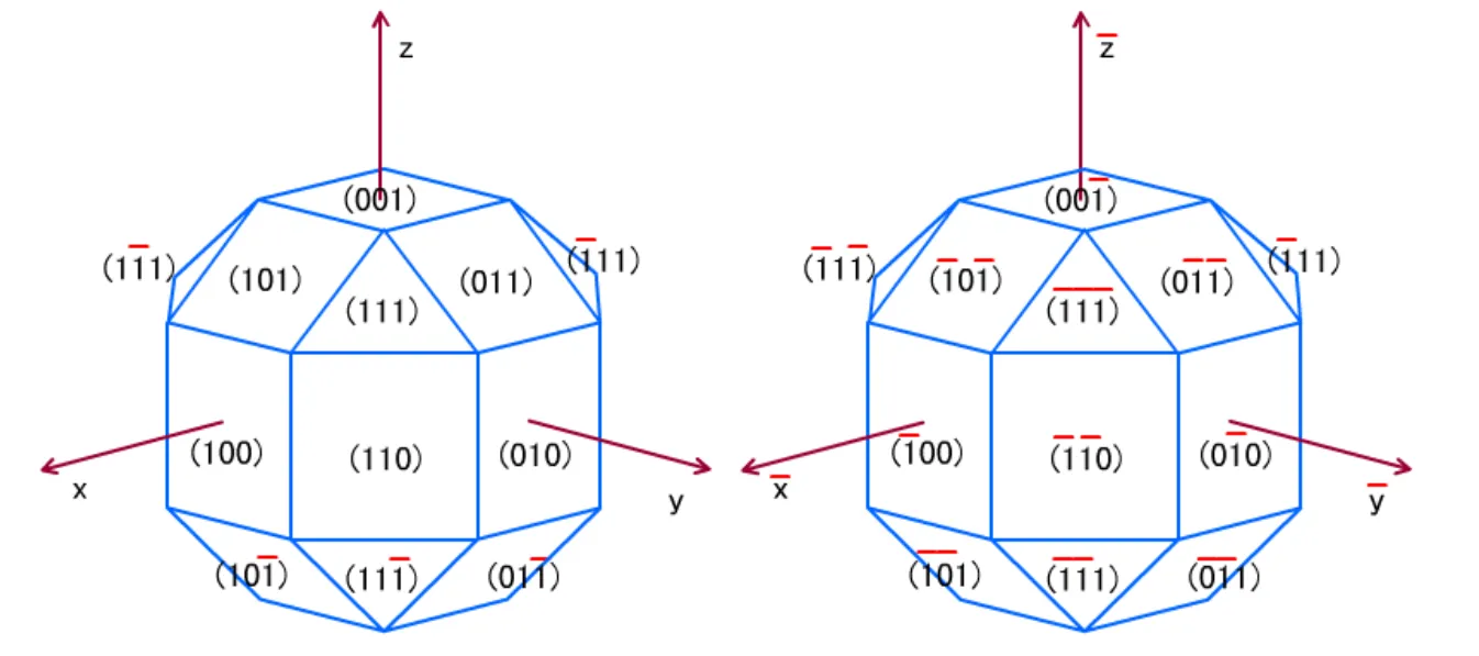 立方晶系中6个等同的{100},12个等同的{110},8个等同的{111}晶面。
Atom density is higher viewed in <100> direction -> lower carrier speed on that plane.
Energy Band
泡利不相容:同一状态(主量子数n+角量子数l+磁量子数m+自旋量子数s)最多被一个费米子占据。费米子:遵循费米—狄拉克统计的粒子。
电子排布:第三层(主量子数n=3)p亚层(角量子数l=1)有2个电子。
。自由空间独立原子,3p层所有轨道在一个能级,3s层在另一个。两个Si原子靠近,形成8个价电子的系统,3p/3s能级分别分裂成两个。N个Si原子组成晶格,3p/3s层各有2N个填充的状态(每个价电子占据一个),形成价带,也各有2N个空状态,形成导带。
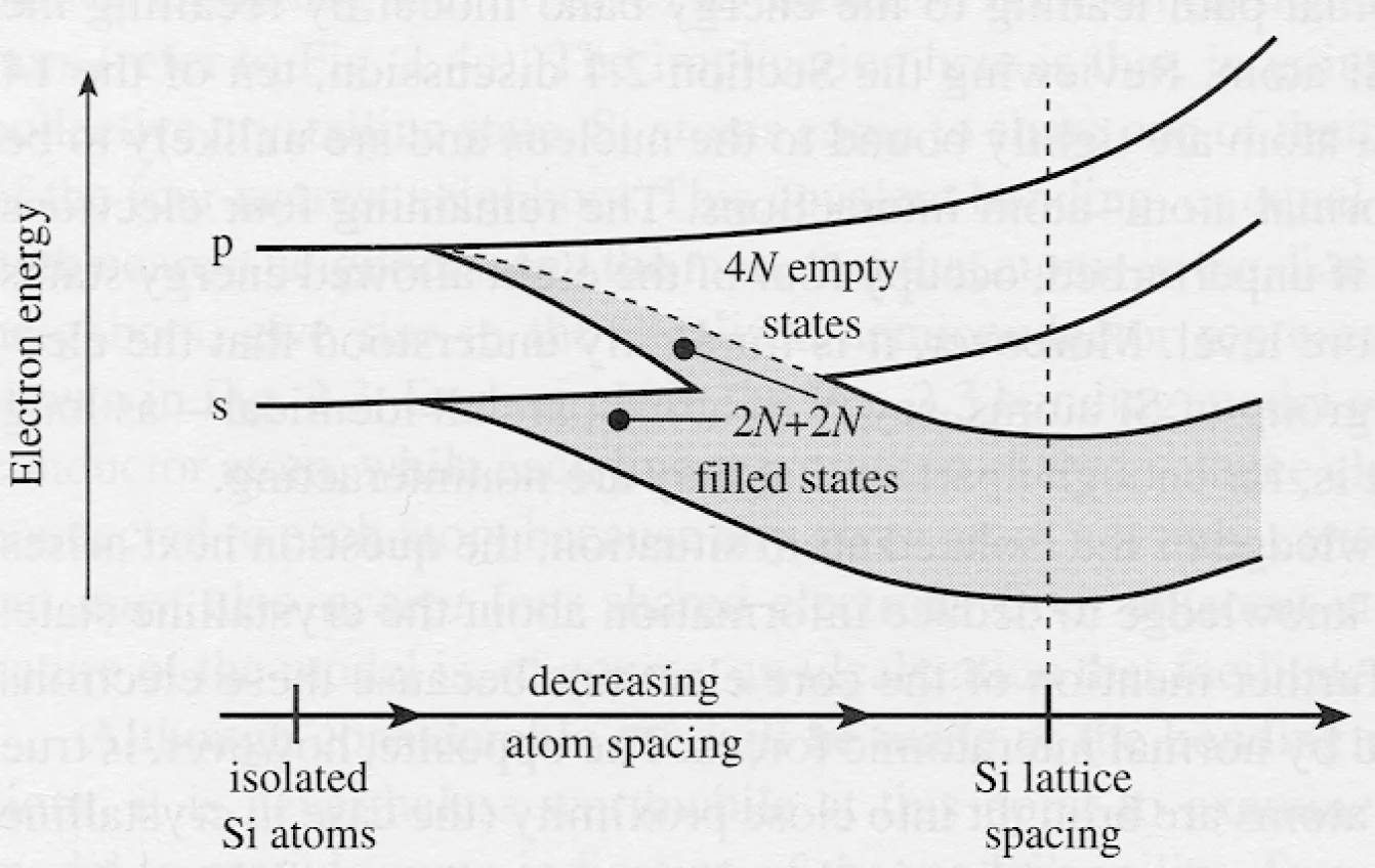
- Valence Band: Highest nearly-filled band.
- Conduction Band: Lowest nearly-empty band
- : Bottom edge of the conduction band.
- : Top edge of the valence band.
- : Separation between and .
Band gap of common materials:
- @ 300K\
- \
- Metals have no band gap (conduction band is partially filled)\
- Graphene = 0\
When temp rises, the lattice transform a little bit, resulting in a changed solution of quantum mechanics, and a shrunk band gap -> temp sensors.
Measurement: minimum energy of photons that is absorbed by the semiconductor. 价带顶电子吸收能量跃迁到导带。
Density of States:
= number of states per cm3 in the energy range between and .
Electron effective mass 电子有效质量,
Concentration of Carriers
To change the concentration of carriers:
- Adding impurity atoms (dopants)
- Applying an electric field
- Changing the temperature
- Irradiation 辐照
Intrinsic (本征) carrier concentration of silicon:
In a pure semiconductor,
In a doped semiconductor, at thermal equilibrium (热平衡状态) Law of Mass Action:
Hole
Mobile positive charge associated with a half-filled covalent bond.
Holes and electrons are not necessarily in pairs. 极子器件.
Doping
Substituting a Si atom with a special impurity atom. (Group III/V)
- Donor ionization energy: Separation between and donor level
- Accepttor ionization energy:
大概几十个meV,随杂质原子序数增大而提高
Donor/acceptor level are close to the or so ionization is easy.
- Ionized donor concentration:
- Ionized acceptor concentration:
- Net dopant concentration:
Charge neutrality condition:
When
- Majority carrier: the most abundant.\
- Minority carrier: the least abundant.
Thermal dynamics
Fermi-Dirac Distribution
The probability that energy level E is occupied. Occupied = by electron, empty = occupied by hole.
There is only one Fermi level in a system at equilibrium (multiple with externel electrical field),
Maxwell-Boltzman Distribution:
简并(Degenerate)半导体:必须用F-D分布,非简并可以用M-B分布。
Summary

- Thermal equilibrium: No external forces, no electric field, no magnetic field, no mechanical stress, no light.