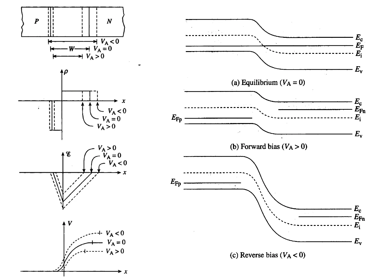
Built-in Potential V b i V_{bi} V bi # Positive charge is left on n-side, and negative on p-side, so the potential on n-side is higher. The electrons in the depletion layer tend to drift to n-side, indicating E c E_c E c
With respect to the uniform E F E_F E F E F − E i E_F - E_i E F − E i E i − E F E_i - E_F E i − E F
q V b i = ( E i − E F ) p − s i d e + ( E F − E i ) n − s i d e qV_{bi} = (E_i - E_F)_{p-side} + (E_F - E_i)_{n-side} q V bi = ( E i − E F ) p − s i d e + ( E F − E i ) n − s i d e
On n-side,
n = n i e E F − E i k T n = {n_i}{e^{\frac{{{E_F} - {E_i}}}{{kT}}}} n = n i e k T E F − E i
( E F − E i ) n − s i d e = k T ln ( n n i ) = k T ln ( N D n i ) \left({E_F} - {E_i}\right)_{n-side} = kT\ln \left( {\frac{n}{{{n_i}}}} \right) = kT\ln \left( {\frac{{{N_D}}}{{{n_i}}}} \right) ( E F − E i ) n − s i d e = k T ln ( n i n ) = k T ln ( n i N D )
similarly,
( E i − E F ) p − s i d e = k T ln ( p n i ) = k T ln ( N A n i ) {\left( {{E_i} - {E_F}} \right)_{p - side}} = kT\ln \left( {\frac{p}{{{n_i}}}} \right) = kT\ln \left( {\frac{{{N_A}}}{{{n_i}}}} \right) ( E i − E F ) p − s i d e = k T ln ( n i p ) = k T ln ( n i N A )
then V b i V_{bi} V bi N D N_D N D N A N_A N A
V b i = k T q ln ( N A N D n i 2 ) {V_{bi}} = \frac{{kT}}{q}\ln \left( {\frac{{{N_A}{N_D}}}{{n_i^2}}} \right) V bi = q k T ln ( n i 2 N A N D )
For p + n \rm p^+n p + n N A , p − s i d e > > N D , n − s i d e N_{A,p-side} >> N_{D,n-side} N A , p − s i d e >> N D , n − s i d e ln ( N D / n i ) \ln\left(N_D/n_i\right) ln ( N D / n i ) N D N_D N D n i n_i n i
V b i = k T q ln ( N A n i ) V_{bi} = \frac{kT}{q}\ln\left(\frac{N_A}{n_i}\right) V bi = q k T ln ( n i N A )
Electric Field in Depletion Layer#
The Depletion Approximation : Charge density on p-side is ρ = − q N A \rho = -qN_A ρ = − q N A ρ = q N D \rho = qN_D ρ = q N D Poisson’s Equation : d 2 V d x 2 = − d E d x = − ρ ε s \frac{{{{\text{d}}^2}V}}{{{\text{d}}{x^2}}} = - \frac{{{\text{d}}E}}{{{\text{d}}x}} = - \frac{\rho }{{{\varepsilon _s}}} d x 2 d 2 V = − d x d E = − ε s ρ
On p-side, letting electric field at x = − x p x=-x_p x = − x p
d E d x = − q N A ε s E ( x ) = − q N A ε s ( x + x p ) \frac{{{\text{d}}E}}{{{\text{d}}x}} = - \frac{{q{N_A}}}{{{\varepsilon _s}}} \qquad E(x) = - \frac{{q{N_A}}}{{{\varepsilon _s}}}\left( {x + {x_p}} \right) d x d E = − ε s q N A E ( x ) = − ε s q N A ( x + x p )
On n-side letting E-field at x = x n x=x_n x = x n
d E d x = q N D ε s E ( x ) = q N A ε s ( x − x n ) \frac{{{\text{d}}E}}{{{\text{d}}x}} = \frac{{q{N_D}}}{{{\varepsilon _s}}} \qquad E(x) = \frac{{q{N_A}}}{{{\varepsilon _s}}}\left( {x - {x_n}} \right) d x d E = ε s q N D E ( x ) = ε s q N A ( x − x n )
The electric field should be continuous at x = 0 x=0 x = 0
N A x p = N D x n {N_A}{x_p} = {N_D}{x_n} N A x p = N D x n
Depletion width of the lightly doped side is narrower.
Electric Potential in Depletion Layer# V ( x ) = V ( x 0 ) − ∫ x 0 x E ( x ′ ) d x ′ V(x) = V({x_0}) - \int\limits_{{x_0}}^x {E(x'){\text{d}}x'} V ( x ) = V ( x 0 ) − x 0 ∫ x E ( x ′ ) d x ′
On p-side, let x 0 = − x p x_0 = -x_p x 0 = − x p V ( − x p ) = 0 V(-x_p) = 0 V ( − x p ) = 0
V ( x ) = q N A 2 ε s ( x + x p ) 2 V(x) = \frac{{q{N_A}}}{{2{\varepsilon _s}}}{\left( {x + {x_p}} \right)^2} V ( x ) = 2 ε s q N A ( x + x p ) 2
On n-side, let x 0 = x n x_0 = x_n x 0 = x n V ( x n ) = V b i V(x_n) = V_{bi} V ( x n ) = V bi
V ( x ) = V b i − q N D 2 ε s ( x − x n ) 2 V(x) = {V_{bi}} - \frac{{q{N_D}}}{{2{\varepsilon _s}}}{\left( {x - {x_n}} \right)^2} V ( x ) = V bi − 2 ε s q N D ( x − x n ) 2
The electric potential should also be continuous at x = 0 x=0 x = 0
q N A 2 ε s x p 2 = V b i − q N D 2 ε s x n 2 \frac{{q{N_A}}}{{2{\varepsilon _s}}}x_p^2 = {V_{bi}} - \frac{{q{N_D}}}{{2{\varepsilon _s}}}x_n^2 2 ε s q N A x p 2 = V bi − 2 ε s q N D x n 2
Depletion Layer Width# With the electric field and electric potential continuity equations, x n x_n x n x p x_p x p
x p = 2 ε s V b i q ( N D N A ( N A + N D ) ) {x_p} = \sqrt {\frac{{2{\varepsilon _s}{V_{bi}}}}{q}\left( {\frac{{{N_D}}}{{{N_A}\left( {{N_A} + {N_D}} \right)}}} \right)} x p = q 2 ε s V bi ( N A ( N A + N D ) N D )
x n = 2 ε s V b i q ( N A N D ( N A + N D ) ) {x_n} = \sqrt {\frac{{2{\varepsilon _s}{V_{bi}}}}{q}\left( {\frac{{{N_A}}}{{{N_D}\left( {{N_A} + {N_D}} \right)}}} \right)} x n = q 2 ε s V bi ( N D ( N A + N D ) N A )
W = x n + x p = 2 ε s V b i q ( 1 N A + 1 N D ) W = {x_n} + {x_p} = \sqrt {\frac{{2{\varepsilon _s}{V_{bi}}}}{q}\left( {\frac{1}{{{N_A}}} + \frac{1}{{{N_D}}}} \right)} W = x n + x p = q 2 ε s V bi ( N A 1 + N D 1 )
Define 1 / N = ( 1 / N A + 1 / N D ) 1/N = \left( 1/N_A + 1/N_D \right) 1/ N = ( 1/ N A + 1/ N D )
For one-sided junction at equilibrium, the built-in potential is determined by the heavily doped side, while the depletion layer width is determined by the lightly doped side.
V b i , p + n = k T q ln N A n i {V_{bi,{{\text{p}}^ + }{\text{n}}}} = \frac{{kT}}{q}\ln \frac{{{N_A}}}{{{n_i}}} V bi , p + n = q k T ln n i N A
W p + n ≅ x n = 2 ε s V b i q N D {W_{{{\text{p}}^ + }{\text{n}}}} \cong {x_n} = \sqrt {\frac{{2{\varepsilon _s}{V_{bi}}}}{{q{N_D}}}} W p + n ≅ x n = q N D 2 ε s V bi
Reversed-Biased PN Junction# The superimposed electric field enhances the built-in electric field, widening the depletion layer.
W = 2 ε s ( V b i + ∣ V r ∣ ) q N W = \sqrt {\frac{{2{\varepsilon _s}\left( {{V_{bi}} + \left| {{V_r}} \right|} \right)}}{{qN}}} W = qN 2 ε s ( V bi + ∣ V r ∣ )
Where V b i + ∣ V r ∣ V_{bi} + \left| V_r \right| V bi + ∣ V r ∣ potential barrier .
Capacitance-Voltage Characteristics# C d e p = A ϵ s W d e p C_{dep} = A\frac{\epsilon_s}{W_{dep}} C d e p = A W d e p ϵ s
1 C 2 = 2 ( V b i + ∣ V r ∣ ) q N ε s A 2 \frac{1}{{{C^2}}} = \frac{{2\left( {{V_{bi}} + \left| {{V_r}} \right|} \right)}}{{qN{\varepsilon _s}{A^2}}} C 2 1 = qN ε s A 2 2 ( V bi + ∣ V r ∣ )
The slope of 1 / C 2 1/C^2 1/ C 2 V r V_r V r N h N_h N h N l N_l N l N l N_l N l V b i V_{bi} V bi V b i V_{bi} V bi N h N_h N h
Peak Electric Field# The peak electric field is at x = 0 x=0 x = 0
E p e a k = E ( 0 ) = 2 q N ε s ( V b i + ∣ V r ∣ ) = 2 ( V b i + ∣ V r ∣ ) W {E_{peak}} = E\left( 0 \right) = \sqrt {\frac{{2qN}}{{{\varepsilon _s}}}\left( {{V_{bi}} + \left| {{V_r}} \right|} \right)} = \frac{{2\left( {{V_{bi}} + \left| {{V_r}} \right|} \right)}}{W} E p e ak = E ( 0 ) = ε s 2 qN ( V bi + ∣ V r ∣ ) = W 2 ( V bi + ∣ V r ∣ )
Breakdown# Given the critical electric field strength of certain material E c r i t E_{crit} E cr i t
V B D = ε s E c r i t 2 2 q N − V b i {V_{BD}} = \frac{{{\varepsilon _s}E_{crit}^2}}{{2qN}} - {V_{bi}} V B D = 2 qN ε s E cr i t 2 − V bi
There are two types of mechanism of breakdown:
Tunneling Breakdown : Dominant if both sides of a junction are very heavily doped.Avalanche Breakdown : Energetic electron cause impact ionization, resulting in a positive feedback. Forward-Biased PN Junction# Apply the forward biasing voltage V A V_A V A V A < V b i V_A < V_{bi} V A < V bi
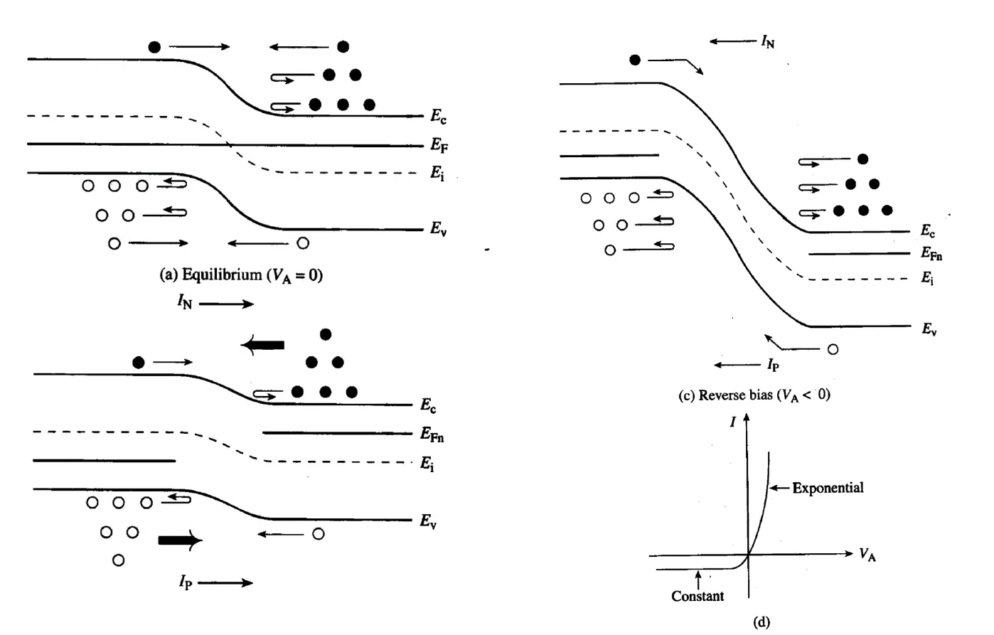
At equilibrium, a small number of electrons on the n-side gains enough energy to overcome the barrier and diffuse to the p-side, but the drifting of the minority electron on p-side balances the diffusion, so no net current.
With a forward bias voltage V A > 0 V_A > 0 V A > 0
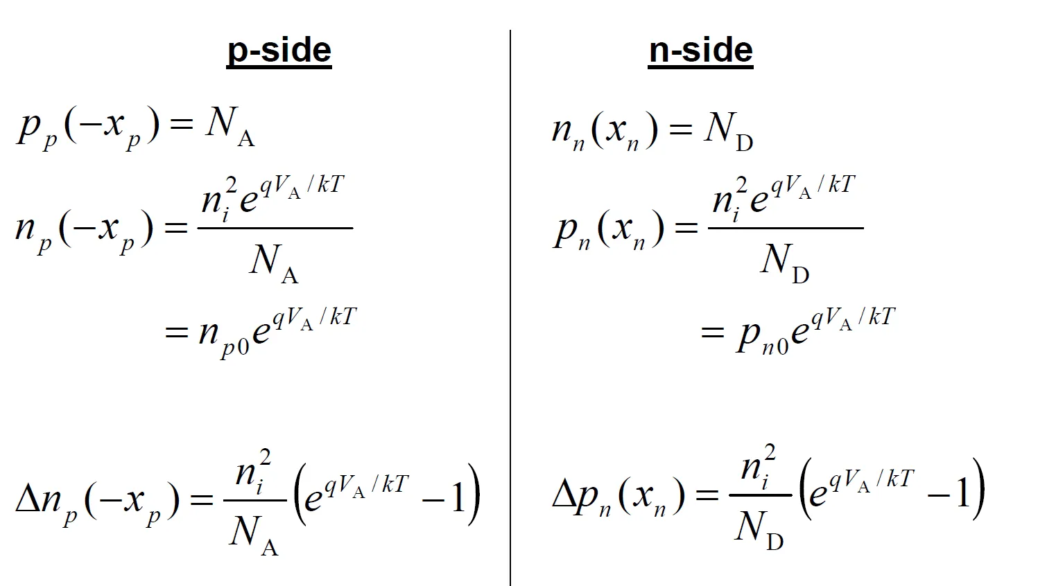
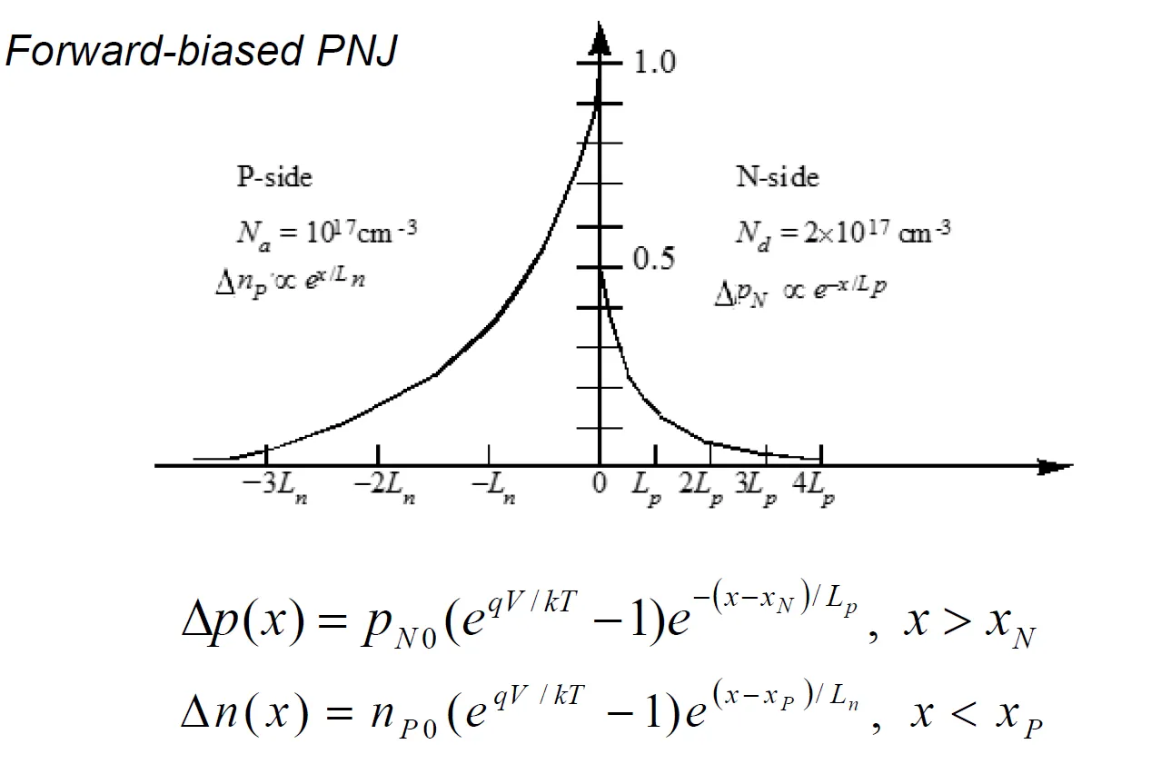
Under low-level injection conditions, the majority carrier concentration at the edge of depletion layer remains the same.
p p ( − x p ) = N A n n ( x n ) = N D {p_p}( - {x_p}) = {N_A} \qquad {n_n}({x_n}) = {N_D} p p ( − x p ) = N A n n ( x n ) = N D
In the depletion layer, the distribution of p p p n n n
p = n i e E i − E F P k T n = n i e E F N − E i k T p = {n_i}{e^{\frac{{{E_i} - {E_{FP}}}}{{kT}}}} \qquad n = {n_i}{e^{\frac{{{E_{FN}} - {E_i}}}{{kT}}}} p = n i e k T E i − E FP n = n i e k T E FN − E i
Although the E F P E_{FP} E FP E F N E_{FN} E FN p n pn p n
p n = n i 2 e E F N − E F P k T = n i 2 e q V A k T pn = n_i^2{e^{\frac{{{E_{FN}} - {E_{FP}}}}{{kT}}}} = n_i^2{e^{\frac{{q{V_A}}}{{kT}}}} p n = n i 2 e k T E FN − E FP = n i 2 e k T q V A
n p ( − x p ) = n i 2 e q V A k T N A p n ( x n ) = n i 2 e q V A k T N D {n_p}( - {x_p}) = \frac{{n_i^2{e^{\frac{{q{V_A}}}{{kT}}}}}}{{{N_A}}} \qquad {p_n}({x_n}) = \frac{{n_i^2{e^{\frac{{q{V_A}}}{{kT}}}}}}{{{N_D}}} n p ( − x p ) = N A n i 2 e k T q V A p n ( x n ) = N D n i 2 e k T q V A
At equilibrium E F N = E F P E_{FN} = E_{FP} E FN = E FP WHAT DOES THAT MEAN?
Minority Carrier Distribution in Quasi-Neutral Region# The minority carriers injected due to V A V_A V A
For excess holes on n-side, the holes flowing out of an element volume is the holes flowing in minus the holes recombined within the volume.
A J p ( x + Δ x ) q = A J p ( x ) q − A Δ x Δ p τ A\frac{{{J_p}(x + \Delta x)}}{q} = A\frac{{{J_p}(x)}}{q} - A\Delta x\frac{{\Delta p}}{\tau } A q J p ( x + Δ x ) = A q J p ( x ) − A Δ x τ Δ p
d J p d x = − q Δ p τ \frac{{{\text{d}}{J_p}}}{{{\text{d}}x}} = - q\frac{{\Delta p}}{\tau } d x d J p = − q τ Δ p
Assuming the minority drift current is negligible,J p = − q D P d p d x {J_p} = - q{D_P}\frac{{{\text{d}}p}}{{{\text{d}}x}} J p = − q D P d x d p
d 2 Δ p d x 2 = Δ p D P τ p = Δ p L p 2 \frac{{{{\text{d}}^2}\Delta p}}{{{\text{d}}{x^2}}} = \frac{{\Delta p}}{{{D_P}{\tau _p}}} = \frac{{\Delta p}}{{L_p^2}} d x 2 d 2 Δ p = D P τ p Δ p = L p 2 Δ p
The boundary conditions are Δ p ( ∞ ) = 0 \Delta p(\infty) = 0 Δ p ( ∞ ) = 0 Δ p ( x n ) = p n ( x n ) − p n 0 ( x n ) \Delta p(x_n) = p_n(x_n) - p_{n0}(x_n) Δ p ( x n ) = p n ( x n ) − p n 0 ( x n )
Δ p ( x ) = p n 0 ( e q V k T − 1 ) e − x − x n L P \Delta p(x) = {p_{n0}}\left( {{e^{\frac{{qV}}{{kT}}}} - 1} \right){e^{ - \frac{{x - {x_n}}}{{{L_P}}}}} Δ p ( x ) = p n 0 ( e k T q V − 1 ) e − L P x − x n
Total Current# The total current density is uniform throughout the junction, and at x n x_n x n J t o t a l = J p N ( x n ) + J n N ( x n ) J_{total} = J_{pN}(x_n) + J_{nN}(x_n) J t o t a l = J pN ( x n ) + J n N ( x n ) J n N ( x n ) = J n P ( − x p ) J_{nN}(x_n) = J_{nP}(-x_p) J n N ( x n ) = J n P ( − x p )
J p N = − q D P d p d x J n P = q D N d n d x {J_{pN}} = - q{D_P}\frac{{{\text{d}}p}}{{{\text{d}}x}} \qquad {J_{nP}} = q{D_N}\frac{{{\text{d}}n}}{{{\text{d}}x}} J pN = − q D P d x d p J n P = q D N d x d n
So the total current is:
J t o t a l = J p N ( x n ) + J n P ( − x p ) = ( q D P L P p n 0 + q D n L n n p 0 ) ( e q V k T − 1 ) {J_{total}} = {J_{pN}}({x_n}) + {J_{nP}}( - {x_p}) = \left( {q\frac{{{D_P}}}{{{L_P}}}{p_{n0}} + q\frac{{{D_n}}}{{{L_n}}}{n_{p0}}} \right)\left( {{e^{\frac{{qV}}{{kT}}}} - 1} \right) J t o t a l = J pN ( x n ) + J n P ( − x p ) = ( q L P D P p n 0 + q L n D n n p 0 ) ( e k T q V − 1 )
Which is proportional to e q V / k T − 1 e^{qV/kT}-1 e q V / k T − 1
I = I 0 ( e q V k T − 1 ) I = {I_0}\left( {{e^{\frac{{qV}}{{kT}}}} - 1} \right) I = I 0 ( e k T q V − 1 )
Where
I 0 = A q n i 2 ( D P L P N D + D N L N N A ) {I_0} = Aqn_i^2\left( {\frac{{{D_P}}}{{{L_P}{N_D}}} + \frac{{{D_N}}}{{{L_N}{N_A}}}} \right) I 0 = A q n i 2 ( L P N D D P + L N N A D N )
The higher the temperature, the higher the current.
Contributions from Depletion Region# The space-charge region current adds a leakage to I I I
I = I 0 ( e q V k T − 1 ) + A q n i W τ ( e q V 2 k T − 1 ) I = {I_0}\left( {{e^{\frac{{qV}}{{kT}}}} - 1} \right) + A\frac{{q{n_i}W}}{\tau }\left( {{e^{\frac{{qV}}{{2kT}}}} - 1} \right) I = I 0 ( e k T q V − 1 ) + A τ q n i W ( e 2 k T q V − 1 )